
Advanced Packaging
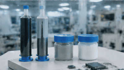
Domestic Substitution Space for Advanced Packaging Materials (Underfill/TIM)
As advanced packaging and heterogeneous integration move from niche capabilities to mainstream semiconductor strategy, materials that once lived quietly in the background are suddenly in the spotlight. Underfill and thermal interface materials, or TIMs, are especially important. They are not glamorous, and they rarely make headlines, but they influence yield, reliability, and thermal performance in some of the most demanding packages being built today. That is why the domestic substitution space for these materials is becoming such a major topic.
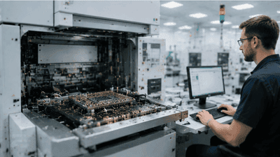
New ATE Requirements from Advanced Packaging: From Single Chip to System-Level
Advanced packaging has changed what it means to test a semiconductor device. For years, automatic test equipment, or ATE, was optimized around a simple idea: validate one chip, one die, one set of pins, one set of failure modes. That world is fading fast. In its place is a much richer and more complicated one, where the “device” under test may be a multi-die package, a chiplet-based module, a 3D stack, or a heterogeneous system built from several process nodes and several vendors.

Hybrid Bonding Transitions from Lab to Fab: 2026 Application Nodes
In 2026, hybrid bonding is crossing a critical threshold: it is no longer just an impressive lab demonstration, but a production-ready enabler for advanced encapsulation and heterogeneous integration. Over the last decade, research consortia, equipment suppliers, and IDMs have steadily refined hybrid bonding processes, addressing alignment, contamination, yield, and reliability challenges. Now, a growing list of products in logic, memory, and mixed-signal domains are starting to rely on hybrid bonding at real application nodes, not just at experimental test vehicles.
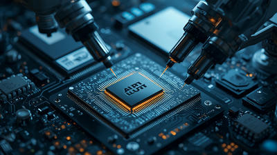
FOWLP Penetration in Mobile AI Chips
Walk into any flagship smartphone launch in 2026 and you will hear three phrases on repeat: on-device AI, power efficiency, and thin design. Hidden behind those buzzwords is a quiet hero in the supply chain: fan-out wafer-level packaging, or FOWLP. Once a niche technology for RF and power management ICs, FOWLP is rapidly finding its way into the heart of mobile AI chips, becoming a key enabler for the performance and form factors consumers now take for granted.

Reliability Testing of Hybrid Bonding Interfaces in 3D-Stacked Memory and Logic
Hybrid bonding has become one of the most important enablers of advanced packaging and heterogeneous integration. It allows memory and logic dies to be joined with extremely fine pitch, low interconnect resistance, and a level of vertical density that traditional micro-bumps cannot match. That technical promise is exciting, but it also raises a hard question: can these interfaces survive real-world operation for years, under heat, stress, and repeated power cycling? Reliability testing is where the answer is found.
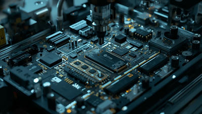
Advanced Packaging’s Share of Total AI Chip Cost Exceeds 30% for the First Time
For the first time, advanced packaging now accounts for more than 30% of the total cost of leading AI chips. What used to be a small, back-end line item has become one of the largest cost buckets alongside high-bandwidth memory and wafer fabrication. This shift is not a statistical curiosity; it is a structural turning point in how AI hardware is built, priced, and constrained. Advanced packaging has moved from the periphery of the semiconductor value chain to its center.
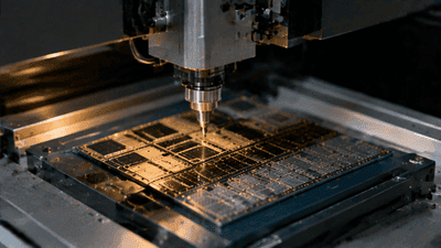
The Advanced Packaging Revolution: Glass Core Substrates vs. Organic Substrates
Walk into any discussion about next-generation AI accelerators or high-performance computing today and you will hear something that would have sounded odd a decade ago: people are arguing about substrates. Not just about die size or node technology, but about what sits under the silicon – glass core substrate or traditional organic substrate. That debate captures a quiet revolution in advanced packaging and heterogeneous integration, as the industry tries to stretch system-level performance without relying solely on transistor scaling.

Panel-Level Packaging (PLP) vs. Wafer-Level (WLP): The Cost Battle
Advanced packaging has become one of the most important battlegrounds in semiconductors, and nowhere is that clearer than in the contest between panel level packaging and wafer level packaging. Both approaches aim to make packages smaller, denser, and more capable of supporting heterogeneous integration, but they do so with very different economics. That is why the PLP versus WLP debate is not just a technical comparison; it is a cost battle that will shape which applications scale fastest in the years ahead.
2027 Advanced Packaging Roadmap: From 3D SoIC to Co-Packaged Optics
The 2027 advanced packaging roadmap is shaping up to be less about a single breakthrough and more about a sequence of tightly linked transitions. On one end sits 3D SoIC, a powerful expression of vertical integration that pushes logic and memory closer together than traditional packaging ever could. On the other end sits co-packaged optics, or CPO, which aims to move the bottleneck of data movement out of electrical interconnect and into the optical domain. Between them lies the broader world of advanced packaging and heterogeneous integration, where chiplets, HBM, hybrid bonding, fan-out, and new substrate technologies are converging into a new system architecture playbook.
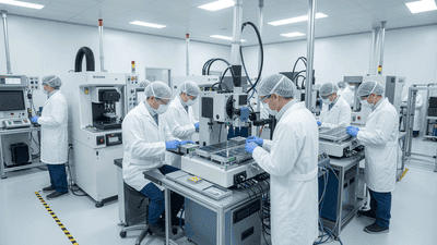
Domestic Progress of Advanced Packaging Tools (Bonders/Molders/Grinders)
If you want to understand how serious a country is about advanced packaging and heterogeneous integration, do not just look at its wafer fabs. Look at its bonders, holders, and the investors behind them. Those quiet, often overlooked tools and capital flows tell you whether the ecosystem is really ready for 2.5D and 3D integration, chiplets, HBM, and all the other buzzwords of the AI era—or whether it is still just talking about them.